
Taiwan Semiconductor Manufacturing Co. has debuted a faster, more efficient logic processing system, dubbed A14, that it claims will support the next generation of artificial intelligence (AI) by combining multiple chips into a single computing device.
Slated to arrive in 2028, these TSMC chip packages will contain semiconductors that are 15% faster and consume 30% less power than its N2 chips, which are planned to start volume production later in 2025.
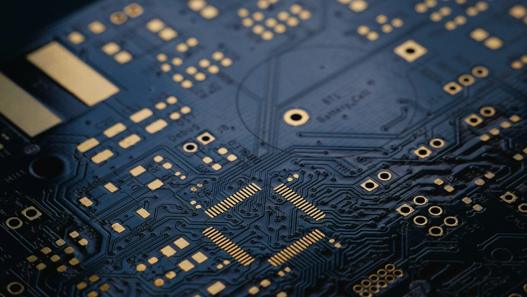
The new TSMC design will combine multiple chips together in a single device at a level never manufactured before. The new design will include up to 16 large semiconductors networked together with ultra-fast optical connections and supported by on-board memory chips. This next-gen configuration will provide thousands of watts of power to drive chip performance.
The 16-chip configuration will be far larger, for example, then NVIDIA’s current top graphics processing units (GPUs), which connect two semiconductors together, and even NVIDIA’s product scheduled for 2027, Robin Ultra, which is expected to contain four chips in one package. The shift to combine chips in addition to fabricating faster chips is driven by the AI market’s voracious demand for compute power. Combining semiconductors is exceptionally complex, and will likely lead to a future chip market where enterprise customers select a chip vendor due to its ability to cater to a buyer’s highly specific requirements.
In addition to its more advanced logic process, TSMC unveiled a number of related innovations. The company is developing its Chip-on-Wafer-Substrate (CoWos) technology, launched in 2024, which supports the high performance computing (HPC) market. For 2027, the company announced plans for a 9.5 reticle size CoWoS to be in full production.
To support the computing power of its recent innovations, TSMC has debuted a new Integrated Voltage Regulator (IVR) for AI that has five times the power density delivery than a separate power management chip on the circuit board. The company also now offers silicon photonics integration with its Compact Universal Photonic Engine, known as COUPE, as well as N12 and N3 logic base die for its HBM4 product, which is produced in partnership with SK Hynix.
To build this vast array of high-tech solutions, TSMC has announced plans to construct two manufacturing plants near its semiconductor fabrication plants in Arizona. The company expects to eventually have a total of 6 facilities, a research center and two packaging plants in the Phoenix area.
These Arizona-based plants will build (or help to build) TSMC’s extraordinary array of recently unveiled innovations. For the smartphone, the company’s N4C RF solution, which is advanced, low-latency wireless connectivity, supports AI on mobile and other edge devices. The company’s N3A fabrication process will enter full production as part a larger suite of technologies for software-defined vehicles.
TSMC as a leading fabricator of high end AI chips contracts with all the leading chip developers, notably NVIDIA and AMD. In recent times, however, the company is facing fresh competition from Intel which, after a long period of struggle, is now set to build its own chip contract business. To support this, Intel is expected to soon unveil its own new manufacturing facilities.
In 2024, Intel touted its plan to displace TSMC as the leader in manufacturing fastest AI semiconductors, but has since, changed course, viewing TSMC more as an ally than a rival. On Thursday, Intel’s new CEO Lip-Bu Tan confirmed meeting with TSMC and having plans to collaborate closely with the chip giant.