
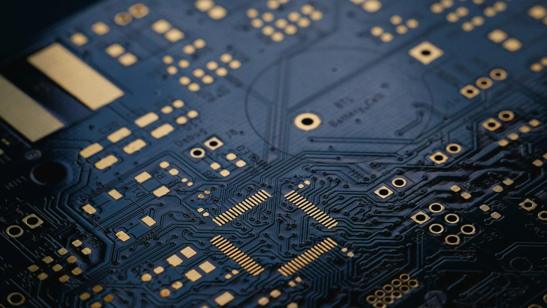
Photonic supercomputing vendor Lightmatter has unveiled two silicon photonic products designed to drive data center connectivity at ultra-fast speeds demanded by today’s artificial intelligence (AI) workloads. The products that transmit signal using light instead of electricity enable faster connectivity mainly because of a design innovation that moves beyond the standard “shoreline” design.
As today’s data centers retool to meet the needs of AI, they face a difficult challenge: Compute performance has greatly surpassed bandwidth scaling. So while the graphical processor units (GPUs) themselves have been architected to process data at remarkably high speeds, the connectivity between points along the signal path is a real bottleneck. This is partially because many legacy connections use electricity instead of optical connections, but even those that use optical units are limited because their I/O interfaces only attach to the edge of the chip, known as the “shoreline.”
Both the new Lightmatter optical products – Passage L200 and Passage M1000 – have evolved past this limitation.
The Passage L200, which Lightmatter touts as “the world’s first 3D co-packaged optics (CPO) product,” integrates with the latest switch silicon and XPU designs (an XPU is a specialized accelerator processor) and according to Lightmatter, offers a 5 to 10x improvement over existing solutions. It is available in both 32 Tbps and 64 Tbps configurations.
The Passage M1000 is a 3D photonic chip built for advanced switches and XPUs. It enables an impressive 114 Tbps optical bandwidth that handles transmission for even the most data-intensive AI workload. The size of the M1000 reference platform, which is over 4,000 square millimeters, enables connectivity with the largest die complexes in a 3D form factor, and—further increasing speed—allows connectivity to thousands of AI-capable GPUs in one domain.
The Passage L200 uses what Lightmatter touts as an “edgeless” I/O that scales bandwidth across the entire die area. It uses a low-power and low-latency UCIe with a photonic integrated circuit (PIC), and its ability to be placed anywhere on the die—instead of just the shoreline—allows it to deliver the bandwidth of 40 pluggable optical transceivers per L200 unit.
“Bandwidth scaling has become the critical impediment to AI advancement,” said Nick Harris, founder and CEO of Lightmatter. “The engineering breakthroughs represented by our L200 family of 3D CPO solutions provide the fundamental building blocks that will pave the way for next-gen AI processors and switches.”
The Passage M1000, employing a similar design strategy, uses an electro-optical I/O that enables connectivity nearly anywhere on the die complex. A reconfigurable waveguide network transmits optical signal across the M1000, which allows what Lightmatter calls “pervasive interposer connectivity.” In sum, this design helps the M1000 support bandwidth that far surpasses conventional CPO (Co-Packaged Optics), even in a smaller form factor.
Lightmatter worked in alliance with GlobalFoundries to build the Passage1000, which includes the GF Fotonix silicon photonics platform to streamline integration of high performance CMOS logic into a single die. This allows the solution to scale as AI workloads require more capacity.
“The M1000 photonic interposer architecture, built on our GF Fotonix platform, sets the pace for photonics performance and will transform advanced AI chip design,” said Dr. Thomas Caulfield, president and CEO of GlobalFoundries. “Our advanced manufacturing capabilities and highly flexible, monolithic silicon photonics solution are instrumental in bringing this technology to market, and we look forward to continuing our close collaboration with Lightmatter.”
Passage M1000 will be available in the summer of 2025, while the L200 chips are scheduled for 2026 availability.